

Top Megasonic Wafer Cleaning Systems for Precision Semiconductor Manufacturing
2026-10-23
In the relentless pursuit of nanometer-scale perfection, even the tiniest particle can render a semiconductor wafer useless. Megasonic cleaning has become the go-to solution for precision surface preparation—but not all systems deliver the same level of control and uniformity. From transducer design to frequency stability, the choices you make here directly impact yield and device reliability. Among the leading options, Siansonic stands out for its engineering focus on high-frequency acoustics and contamination-free processing. In this article, we’ll break down the top megasonic wafer cleaning systems and the key factors that separate a good clean from a great one.
Why 3 nm Yield Hinges on Cavitation Control, Not Just Clean Chemistry
At 3 nm, cleaning steps that once felt routine now decide whether a wafer leaves the fab with 60% or 90% good die. People tend to fixate on bath composition, pH, surfactant loading. But the real spoiler is cavitation: the formation and collapse of tiny vapor bubbles in cleaning fluids. A collapsing bubble near a fin or gate-all-around structure can punch out a few nanometers of material, create pits, or snap a high-aspect-ratio feature that survived etch. It is not a chemistry problem; it is a mechanical one.
Traditional megasonic cleaning relied on stable cavitation to loosen particles, but at these dimensions the margin between useful agitation and structural damage nearly vanishes. Transient cavitation events can be rare yet still lethal. One violent collapse per million cycles is enough to kill a wafer full of 3nm transistors. So fabs now have to map acoustic pressure fields, tune frequency and dissolved gas levels, and run particle removal efficiency tests alongside damage monitors. The chemistry can be perfect and the rinse spotless, but if the cavitation window is wrong, yield drops without an obvious chemical trace.
This is why process engineers talk about cavitation control as its own variable, not a footnote in clean chemistry. Gas concentration, temperature ramps, nozzle geometry, and power density matter as much as the cleaning formula itself. A solution that works at 5nm can tear through 3nm structures simply because the features got weaker while the bubbles stayed the same.
Protecting Thinned Wafers from Acoustic Damage During Final Clean
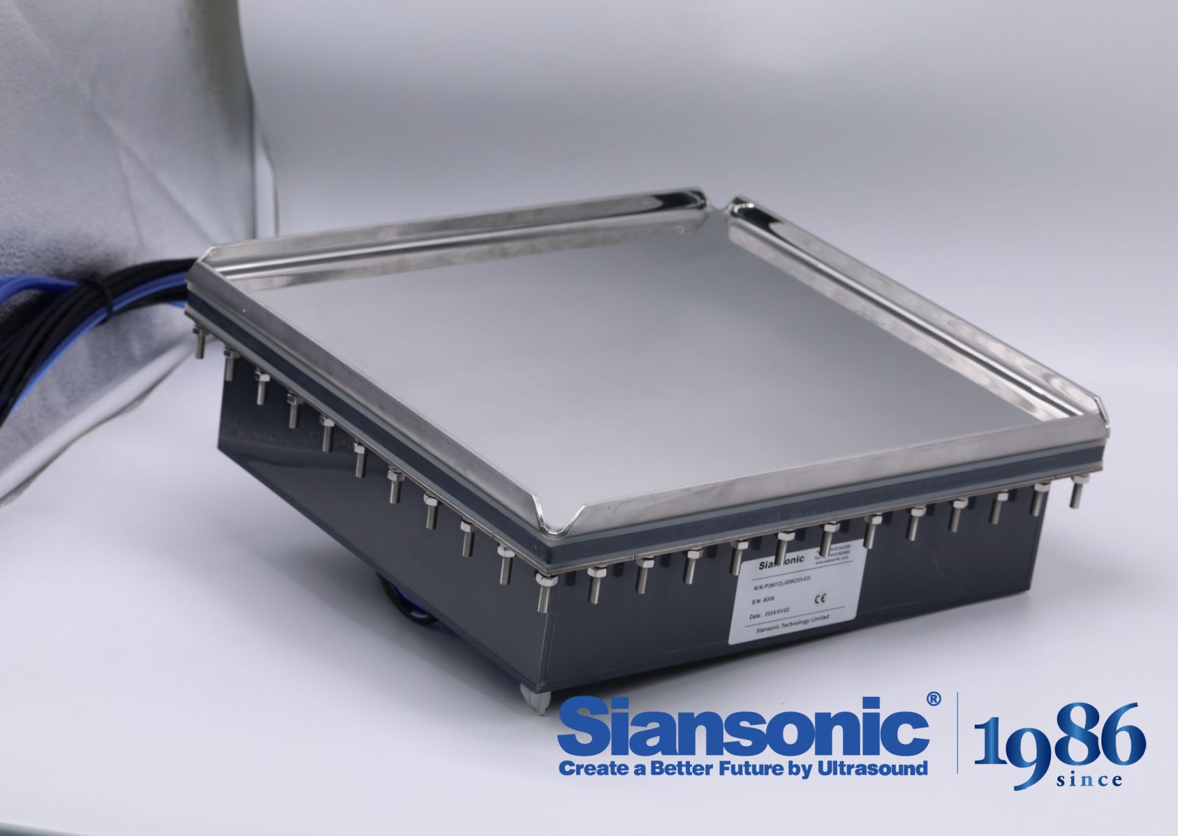
Wafer thinning pushes silicon into a regime where acoustic energy, typically considered gentle for standard substrates, can become a source of micro-fractures. The final clean step often relies on megasonic agitation to dislodge particles, but the same pressure waves that remove contaminants can propagate through an ultra-thin wafer and concentrate stress at existing micro-cracks or edge defects. The result is a yield loss that shows up not during cleaning but later during die attach or wire bonding.
One practical safeguard is to lower the acoustic power density while extending the clean time slightly, keeping cavitation energy below the threshold that triggers crack growth. Equipping the cleaning tank with a softer transducer array or using pulsed megasonic bursts instead of continuous wave operation distributes the mechanical load more evenly. In parallel, gentle wafer support becomes critical: a full-contact chuck or a flexible carrier with vibration-damping edges prevents the wafer from resonating like a drumhead.
Process monitoring should track not only particle removal efficiency but also acoustic intensity at the wafer surface, ideally via a sacrificial monitor wafer with embedded strain sensors. Some fabs introduce a short, low-energy rinse before the main clean to stabilize the thinned wafer, while others replace the final megasonic step with a high-flow, low-pressure spray for sensitive products. The key is to match the acoustic profile to the wafer's residual stress, something that cannot be left to a one-size-fits-all recipe.
The Cost of Ignoring Bath Contamination in Mixed-Product Lines
Operators often learn to live with shared bath lines because switching chemistries for every part number feels impractical. That tolerance has a price. Drag-in from one substrate, brightener breakdown from another, and airborne shop debris accumulate until the bath no longer behaves the same at 2 p.m. as it did at 7 a.m. The first visible signs are usually dull patches, uneven thickness, or adhesion failures that get written off as one-off defects. By the time the pattern is obvious, several batches have already shipped with borderline quality.
The less visible costs hurt more. Mixed-product contamination forces frequent titrations, longer inspection holds, and unplanned bath adjustments that eat into production windows. Rework and scrap rise quietly, but capacity takes the bigger hit because every corrective action interrupts the line. A bath that drifts out of spec also ages faster, so replacement and waste treatment costs climb. In a mixed-product environment, ignoring contamination doesn't create a single catastrophic event; it creates slow, compounding losses that show up in overtime, missed delivery dates, and customer returns.
Single-Wafer Megasonics and the Battle Against Edge Exclusion
The move to single-wafer megasonic cleaning arose from the need to control energy delivery at the wafer's periphery, where batch immersion tools leave a stubborn band of under-cleaned surface. In theory, megasonic agitation dislodges nanoparticles through cavitation and acoustic streaming; in practice, the wafer edge interrupts the acoustic field, creating a dead zone that stubbornly resists uniform particle removal. Single-wafer platforms attack this by directing a focused transducer across the surface with a thin chemical film, letting the acoustic energy sweep past the bevel instead of bouncing off a tank wall.
But the battle is far from won just by changing the hardware. Edge exclusion—the few millimeters from the wafer rim that device makers often write off as unusable—becomes a contested zone when advanced packaging and 3D integration squeeze usable silicon closer to the edge. Process engineers now tune megasonic power, scan speed, and nozzle angle specifically to extend cleaning into that exclusion band without damaging fragile edge structures. Too much energy at the bevel can peel back dielectric films or chatter through thin device layers; too little leaves residues that migrate inward during subsequent etch or deposition.
The real breakthrough is not a single setting but a feedback loop. Modern single-wafer tools map acoustic intensity at the edge using sacrificial wafers or embedded sensors, then adjust the transducer path to compensate for the drop-off near the rim. Some fabs pair the megasonic step with a low-flow edge rinse that drags chemistry across the boundary instead of relying on bulk acoustic force alone. The result is a quieter, more deliberate fight against edge exclusion—one that trades the brute force of batch cavitation for a targeted sweep that respects the wafer's most vulnerable millimeters.
Transducer Aging and Its Hidden Effect on Cleaning Uniformity
Over time, the piezoelectric elements inside ultrasonic transducers lose their ability to vibrate at the original calibrated frequency. This drift is rarely sudden; it accumulates through thousands of hours of operation, driven by thermal cycling, mechanical fatigue, and gradual depolarization of the ceramic material. What makes this aging process particularly deceptive is that the generator may still display normal power readings, leading operators to believe the cleaning tank is performing at full capacity.
The hidden effect emerges in the distribution of cavitation energy across the liquid volume. As individual transducers age at slightly different rates, the acoustic field becomes uneven, creating zones of intense cleaning next to areas that barely receive any energy. Parts positioned in these weak spots emerge with residual contamination, even though the overall process parameters remain unchanged from the original validation.
Detecting this non-uniformity requires more than periodic visual inspection of the tank surface. Mapping the cavitation intensity with a hydrophone or foil erosion test reveals the real story: a patchwork of energy levels that shifts as the transducers continue to age. Ignoring this silent degradation leads to unpredictable cleaning results and, eventually, a sudden spike in rejected parts that cannot be traced back to any single process change.
Rethinking Frequency Selection for High-Aspect-Ratio Trench Cleaning
The conventional logic for selecting acoustic frequency during high-aspect-ratio trench cleaning leans heavily on cavitation bubble resonance and particle-removal thresholds. But inside narrow, deep structures, that framework quickly breaks down. The trench acts as a waveguide, filtering out certain frequencies and creating standing-wave patterns that push debris into corners rather than lifting it out. Rethinking frequency selection means treating the trench geometry as the primary filter, not the contaminant size.
A more useful approach starts with measuring the acoustic impedance mismatch between the cleaning fluid and the trench walls. At lower frequencies, the long wavelength tends to create uniform but weak pressure oscillations along the depth; at higher frequencies, the energy stays near the opening and fails to reach the bottom. There is a middle band—often higher than conventional megasonic ranges for very deep trenches—where the fluid inertia matches the restoring force of the trapped gas or liquid column. Selecting a frequency near that band improves penetration without relying on bulk cavitation.
Some process teams are now using pulse trains with frequency hopping to avoid persistent nodes. Instead of holding a single frequency that may align with a harmonic of the trench depth, they sweep through a narrow range to keep the pressure antinodes moving. This prevents the build-up of compacted residue at fixed points along the sidewall. The result is a cleaning process that works with the acoustic modes of the trench rather than against them, allowing high-aspect-ratio features to be cleared more consistently.
FAQ
The transducer creates pressure waves in the liquid, typically between 0.8 and 3 MHz. Those frequencies are high enough to keep cavitation bubbles in a controlled, non-collapsing state. Instead of violent implosions, you get steady microstreaming and acoustic pressure gradients that gently roll particles off the surface. That is why it works well on patterned wafers where aggressive ultrasonic energy would tear fine lines.
At megasonic frequencies the cavitation threshold is much higher, so the energy stays below the point of bubble collapse. The cleaning action comes from acoustic streaming and the drag force it exerts on boundary layers. Tiny particles lodged in trenches see enough shear to dislodge, while the structure itself does not experience hammering. Process optimization with dissolved gas control is still critical, because too much gas can lead to unstable cavitation.
Dissolved gases like nitrogen or oxygen lower the cavitation threshold, which changes the cleaning mechanism. Some fabs intentionally degas the solution to suppress bubble activity and rely purely on acoustic streaming for damage-sensitive layers. Others inject a controlled gas concentration to get gentle, stable cavitation that boosts particle removal. The choice often depends on the film stack and feature geometry.
The transducer array design is probably the first thing to evaluate, because it determines uniformity across the wafer. After that, look at frequency control, power density, and whether the tool supports single-wafer or batch processing. You also need robust temperature control and chemical compatibility with the cleaning chemistries already in use. A system that can log energy delivery per wafer is a plus for traceability.
It is used across the flow, but the recipe changes. On metal layers you typically run at lower power density and higher frequency to avoid electromigration or corrosion issues. Some fabs also switch to degassed chemistries to reduce the chance of micro-damage on soft metals like aluminum or copper. The key is matching the acoustic energy to the material's mechanical sensitivity.
Single-wafer systems give you tighter process control and better uniformity for 300mm wafers, which matters when chasing defect densities below 0.1 per square centimeter. Batch systems still have an edge in cost per wafer for some mature nodes or less critical cleans. The trend in leading fabs is toward single-wafer megasonic modules integrated with other wet clean steps so the wafer never leaves the controlled environment.
Dilute chemistries reduce surface roughness and material loss while the acoustic energy provides the physical removal force. That combination lets you keep etch rates very low, which is essential for 3D structures and thin films. It also cuts chemical consumption and waste treatment costs compared to concentrated baths.
Conclusion
Anyone chasing yield at 3 nm quickly learns that clean chemistry alone is a weak defense. The real battle is cavitation control: uncontrolled bubble collapse can fracture ultra-thin gate stacks or leave latent damage that shows up only at probe. Thinned wafers used in advanced packaging make this even harder, since final clean must remove particles without sending acoustic stress into a substrate that may be only tens of microns thick. In older bath-style megasonic tools, mixed-product lines add another layer of risk. Bath contamination from one device lot can carry metallic or organic residues into the next, and shared chemistry tends to erode edge yield. Moving to single-wafer megasonic systems addresses both problems. The energy can be directed locally, edge exclusion becomes a controlled variable rather than a compromise, and cross-lot contamination drops sharply because there is no shared reservoir to clean.
Transducer aging quietly undermines all of this. As piezoelectric elements age, they drift in frequency and amplitude, so a recipe that cleaned uniformly last quarter may now leave dead zones or over-stress the wafer edge. Acoustic mapping at periodic maintenance is not optional if you want repeatable cleaning. For high-aspect-ratio trench structures, the frequency question becomes equally nuanced. Standard 1 MHz or 40 kHz settings are rarely optimal. Deep, narrow trenches need enough energy to reach the bottom, but too much low-frequency cavitation can collapse the sidewalls. Leading systems now pair frequency sweeping or pulsed megasonic delivery with real-time cavitation sensors, allowing the tool to adjust energy based on feature geometry and wafer thickness. That kind of closed-loop control is what separates a generic wet cleaner from a precision megasonic system capable of supporting next-generation semiconductor manufacturing.
Contact Us
Contact Person: Ivy Zhang
Email: [email protected]
Tel/WhatsApp: +86 1081502288
Website: https://www.siansonic.com/